Spending Moore's dividend
Parallel Visions
The IT industry's remarkable progress over the past half century has been fueled by a simple fact that was codified in 1965 by Intel co-founder Gordon Moore in his eponymous law [1]. The number of transistors in an integrated circuit doubles every two years. This law is explained by constant advances in the manufacturing process, which over time have reduced the size of a single transistor to the nanometer scale and enabled ever-increasing speeds. The original Intel 8086 microprocessor sported 29,000 transistors and clocked at a then-blistering 5MHz; 28 years later, the 2.93GHz Intel Core 2 Duo boasted an impressive 291 million transistors, 10,034 times the original [2].
The first CPU to break the 3GHz barrier was an Intel Pentium 4 variant released in 2002 [3], but disregarding unreliable overclocking speeds or IBM's 5.5GHz liquid-cooled mainframe processor [4], the top clock speed has been hovering between 3 and 4GHz for the past 11 years. Power dissipation physics has put a limit on what can be done in terms of pure clock speed, yet Moore's law continues unabated, which poses the interesting question that James Larus concisely framed years ago as "spending Moore's dividend."
Transistors, Transistors, Everywhere
Early beneficiaries of transistor gains that could no longer be spent in traditional approaches have been cache sizes. This development has helped alleviate the yawning speed gap between a CPU and the RAM feeding it instructions and data to process. The Von Neumann bottleneck limits a CPU's actual usable speed, as instruction-fetch stalls and data-cache misses can force the CPU to wait for the slower subsystem to deliver more work to it. Bigger caches make this outcome less likely.
More ambitious approaches to spending the dividend also materialized in the form of video cards evolving into today's GPU hardware. This vision of computing revolves around highly parallel single-instruction, multiple-data (SIMD) algorithms applied to problems that can be suitably partitioned, such as the rendering of a 3D scene.
The current apex of this development path is the NVidia Tesla K20X, which delivers a staggering 1.31 teraFLOPS of double-precision number-crunching performance. This performance is accomplished with 2,688 CUDA cores on a single expansion board [5], which is three times as efficient in performance-per-watt terms as the preceding Tesla Fermi design and consumes 225 watts at peak power. If you can fit your problem into the CUDA or OpenCL parallelism model, this option can be very attractive.
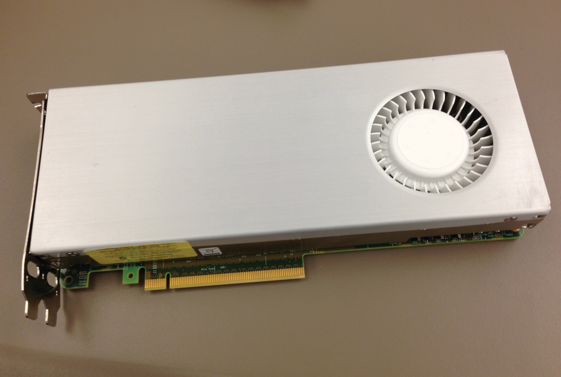
A divergent yet equally powerful vision is Intel's Xeon Phi coprocessor – better described as a Linux cluster in a single expansion card [6]. The Intel design is essentially a symmetric multiprocessor on a single chip die. The Xeon Phi 5110P, code-named "Knights Corner" [7], features 60 x86 cores in the same 225-watt power envelope at a price comparable to the NVidia Kepler GPU (Figure 1). What is really different is the programming model: The cores are running a custom distribution of Linux and work together as a cluster in a multiple-instruction, multiple-data (MIMD) fashion.

The cores are an in-order-execution variant of the x86 architecture that Intel refers to as many integrated core (MIC, read "mike") [8]. The advantage of Intel's design is that the model is more familiar to developers of multithreaded applications and does not require as drastic an algorithm change as the NVidia model. What draws my interest to this model is that many optimizations that must be carried out to improve performance on the Phi will also benefit the same program if run on a multicore Xeon system – an important synergy in terms of developer time and learning curve.
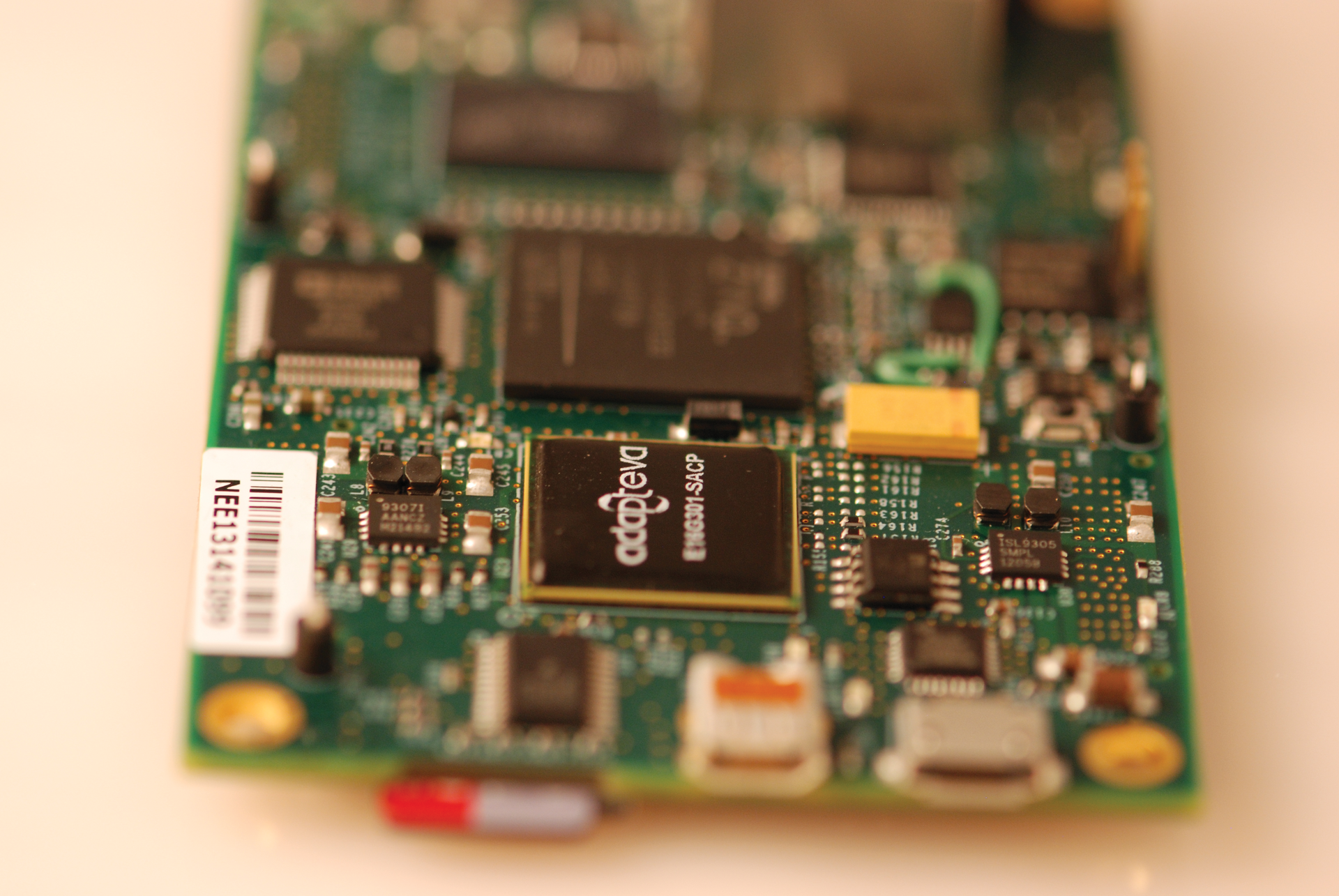
An unexpected new entrant in the mindshare competition for Moore's dividend is Adapteva, a startup that has designed, manufactured, and documented the Epiphany [9] architecture of numerical acceleration cores. A very successful crowd-funding campaign financed the mass-production of silicon for the Parallella open hardware board [10] released in July (Figure 2). The Parallella is effectively designed like a supercomputer, with a host-side, dual-core Zynq-7010 ARM A9 CPU running Ubuntu 12.04, flanked by a 16-core Epiphany accelerator running at 700MHz. Priced at US$ 99, as opposed to the thousands of dollars of the other two designs, the Parallella board is powered by a mere 5 watts and requires no external cooling.

Adapteva has open-sourced the toolchain necessary to program the accelerator, and the Gigabit Ethernet interface onboard promises tantalizing cluster possibilities – the team has already demonstrated a 756-core cluster, powering 42 boards with less than 500 watts [11]. As Adapteva perfects its 64-core silicon design and a community of users forms (the crowd-funding campaign promises to deliver more than 6,000 boards to users), a new open hardware player might just join the two hardware giants in the fray.
